0 PrefaceRed copper has good ductility, high thermal conductivity, and electrical conductivity, and is widely used in aerospace, marine engineering, cable and electrical, and electronic components.Traditional red copper welding methods such as tungst...
Contact Us
0 Preface
Red copper has good ductility, high thermal conductivity, and electrical conductivity, and is widely used in aerospace, marine engineering, cable and electrical, and electronic components.Traditional red copper welding methods such as tungsten inert gas welding have high heat input, large post-welding deformation, and unsightly weld seams, which can no longer meet the requirements of modern production.
Laser welding has less overall heat input, which can greatly improve the problems of large post-welding deformation and poor appearance. The laser welding technology has developed rapidly in recent years.Due to the low absorption rate of near-infrared wavelength lasers on the copper surface, generally only about 4%, most of the laser energy is reflected away. It requires high energy input to weld copper, which could lead to poor welding stability;During the melting process of red copper, pores are easily formed at the weld seam, which affects the mechanical properties of the weld joint;When welding red copper, the large heat input leads to a drastic increase in grain size, which also adversely affects the performance of the welded joint;
The new semiconductor and fiber laser composite welding technology is used in the experiment to laser weld red copper. The influence of process parameters on the weld joint formation is analyzed to provide technical references for actual production.
1 Welding experiment
1.1 Materials to be welded and welding equipment
The experimental material is red copper, with a thickness of 1.0 mm, length × width of 100mm×50mm. The welding method is splicing. The material to be welded is clamped with a homemade fixture to reduce deformation during welding.
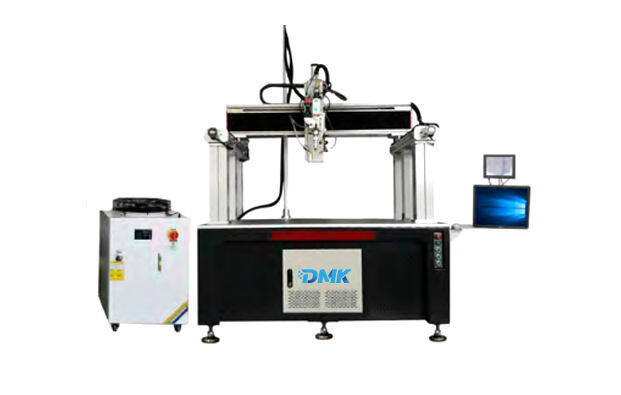
A composite laser of a semiconductor laser and a fiber laser are used to weld red copper. The wavelength of the semiconductor laser is 976nm, the maximum power is 1000W, and the core diameter of the fiber is 400 microns.The fiber laser has a wavelength of 1070nm, a maximum laser power of 1000W, and a fiber core diameter of 50 microns. The two types of lasers are combined through a welding head, with the collimation lens of the welding head having a focal length of 100mm and the focusing lens having a focal length of 200mm,the optical path is shown in Figure 1(a),the spot diameter of the semiconductor laser after passing through the welding head at the laser focus is about 0.8mm. Due to the large spot size, it can provide auxiliary heating around the weld seam.The spot diameter of the fiber laser at the focus is about 0.1mm, and the power density is small (power density = laser power/spot area; the smaller the spot diameter, the greater the power density). This can generate higher temperatures, achieving the welding of copper materials.All the experiments mentioned in the text were conducted at the focal points of semiconductor lasers and fiber lasers for welding.The laser composite welding experimental platform is shown in Figure 1(b). It mainly consists of a semiconductor laser, a fiber laser, a welding head, an industrial control computer and an X/Y module. In this setup, the welding head, driven by the X/Y module, achieves track welding to form a weld seam. The power of the semiconductor laser and fiber laser can be set separately.
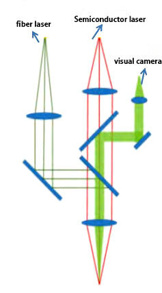 (a) Schematic diagram of hybrid welding optical path |
 (b) Experimental equipment |
|
Figure 1 Laser welding equipment |
|
1.2Weld inspection equipment
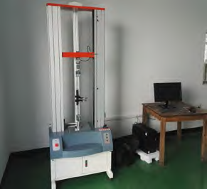
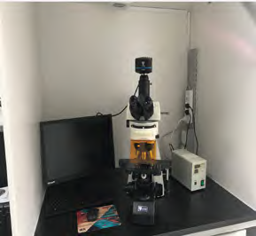
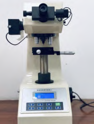
The weld seam microstructure was tested and analyzed using a metallographic microscope, model WYJ-4XBD. This was done to analyze the effects of different process parameters on the weld seam microstructure.The tensile strength of the weld seam was tested using an electronic tensile machine, model FR-103C. The equipment is shown in Figure 2(b).The tensile strength P of the weld seam is obtained by dividing the tensile force F by the area S of the weld seam. The tensile strength is tested 3 times under each process parameter, and the average tensile strength obtained is the tensile strength of the weld seam corresponding to this process parameter. The stretch speed of the tensile machine is set to 1mm/s.The microhardness of the welded seam joint of the weld sample is tested with a microhardness tester, model HV-1000. The experimental load is 50g, and the loading time is 10s.
|
(a) Weld tensile strength testing instrument |
(b) Weld microstructure testing equipment |
(c) Weld microhardness tester |
|
Figure 2 Weld testing equipment |
||
2 Experimental process and result analysis
2.1 Effect of semiconductor laser on the appearance and strength of welds
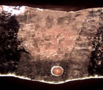
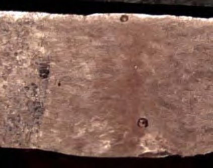
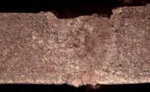
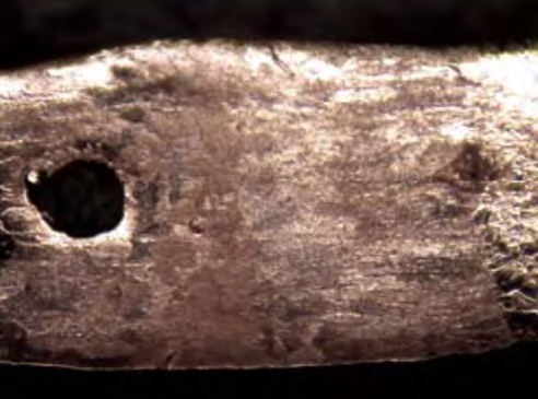
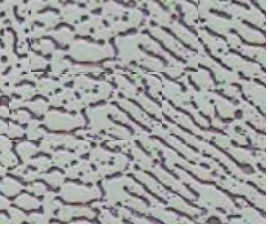
After numerous preliminary experiments, when using only a fiber laser for welding (with the semiconductor laser power set to 0W), if the power of the fiber laser is 900W and the welding speed is 30mm/s, the weld seam will just penetrate, but it is prone to pore formation inside the weld seam.As shown in Figure 3(a),in continued attempts to optimize process parameters such as welding speed and laser power for fiber laser welding, there are still pores inside the weld seam. This is because during the melting process of purple copper, the fiber laser has a large heat input to the copper and a high temperature, which greatly increases the solubility of hydrogen in the air in the molten pool.At the same time, due to the good thermal conductivity of purple copper, the cooling speed of the molten pool is very fast. The quick solidification of the molten pool causes the hydrogen dissolved in the molten pool to not dissipate from the weld seam in time, resulting in residual hydrogen inside the weld seam and the formation of pores in the seam. These internal pores in the weld seam will adversely affect the mechanical properties of the weld joint.
The article employs a composite welding method using a semiconductor laser and a fiber laser. The power of the fiber laser is kept constant at 900W and the welding speed at 30mm/s. The power of the semiconductor laser is set at 600W, 800W, and 1000W respectively to analyze the effect on the weld seam. When the power of the semiconductor laser is 600W, the weld seam shown in Figure 3(b), there are pores present within the weld seam.When the power of the semiconductor laser is 800W, as shown in Figure 3(c), there are no pores within the weld seam. This is because the semiconductor laser has a spot diameter of 0.8mm at the focal point, covering a larger heating range. The semiconductor laser provides auxiliary heating around the weld seam, which reduces the cooling rate of the molten pool. This allows the hydrogen dissolved in the molten pool sufficient time to evaporate from the weld seam, leaving no residual pores in the weld seam.When the semiconductor laser power is further increased to 1000W, the appearance of the weld seam is as shown in Figure 3(d), with larger pores inside. This might be due to the excessively high power of the semiconductor laser, leading to larger overall heat input. This causes ablation of low-melting-point elements within the copper and leaves cavities within the weld seam.
|
(a) The semiconductor laser power is 0W |
(b) The semiconductor laser power is 600W |
|
(c) The semiconductor laser power is 800W |
(d) The semiconductor laser power is 1000W |
|
Figure 3 Cross-section view of weld |
|
The tensile strength of the weld seam is tested using a tension testing machine,when the parameters of the fiber laser power are set at 900W, the welding speed at 30mm/s, and the defocus amount at 0mm are kept constant, an analysis of the impact of semiconductor laser power on the tensile strength of the weld seam is conducted, with results presented in Figure 4.When the semiconductor laser power is set at 0W and 600W, there is no significant change in the tensile strength of the weld seam. This is because a power of 600W does not have a significant impact on the morphology of the weld seam. Similar to when the power is at 0W, there are pores produced inside the weld seam, resulting in a tensile strength between 160~161MPa.When the semiconductor laser power is set at 800W, the tensile strength of the weld seam reaches its highest at 238MPa, achieving 80% of the copper base material's tensile strength (which is 292MPa). This represents an increase of about 50% in tensile strength compared to when the semiconductor laser power is set at 0W and 600W.When the semiconductor laser power is set at 1000W, the tensile strength of the weld seam dramatically decreases. This occurs because the semiconductor laser power is too high, causing the low-melting-point elements to be ablated, drastically reducing the tensile strength of the weld seam.
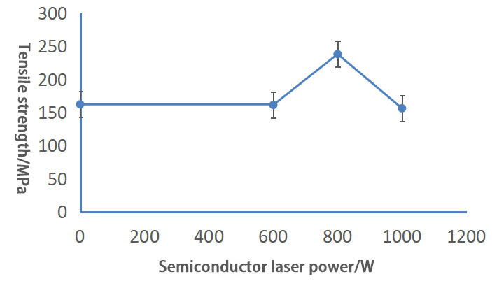
Figure 4 Tensile strength of welded joints under different semiconductor laser powers
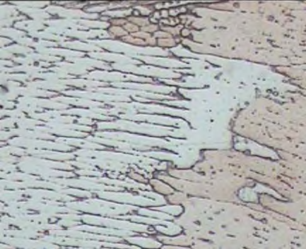
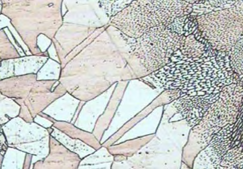
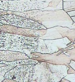
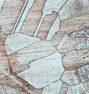
2.2 Effect of semiconductor laser on weld microstructure
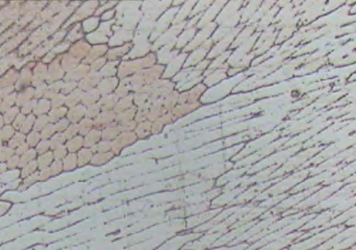
With a power of 900W, the fiber laser welder operates at a speed of 30mm/s, with 0mm of defocus. The microstructure metallographic images of the fusion zones at different semiconductor laser powers are shown in Figure 5. When the semiconductor laser power is set at 0W, the microstructure of the fusion zone is a slender cellular crystal structure, as shown in Figure 5(a). When the semiconductor laser power is set at 600W and 800W, the microstructures of the fusion zones are shown in Figure 5(b) and Figure 5(c), respectively. With the increase in semiconductor laser power, the cellular crystal structure gradually becomes coarser. This is because the temperature gradient in the fusion zone is relatively large, the grains grow in the direction of heat conduction, forming fine cellular crystal structures.When the semiconductor laser power is set at 1000W, the microstructure of the fusion zone, as shown in Figure 5(d), transforms into a much coarser α-Cu structure. This is due to the extremely slow cooling rate, resulting in the formation of large α-Cu grains.
|
(a) The semiconductor laser power is 0W |
(b) The semiconductor laser power is 600W |
|
(c) The semiconductor laser power is 800W |
(d) The semiconductor laser power is 1000W |
|
Figure 5 Microstructure of the fusion zone under different semiconductor laser powers |
|
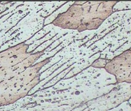
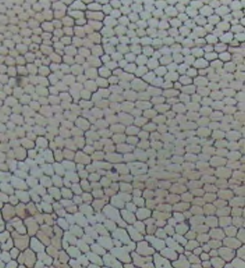
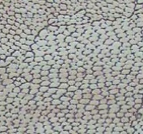
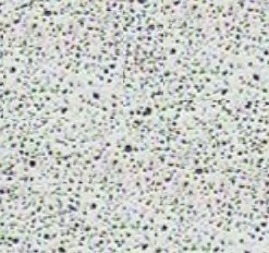
With a power of 900W, the fiber laser welder operates at a speed of 30mm/s, with 0mm of defocus. The microstructure metallographic images of the heat-affected zones at different semiconductor laser powers are shown in Figure 6. The structure of the heat-affected zones is all annealed α-Cu.When the semiconductor laser power is set at 0W and 600W, the grain sizes in the heat-affected zone do not vary significantly, as shown in Figure 6(a) and Figure 6(b). This is due to the relatively low power of the semiconductor laser, which does not have a noticeable effect on the microstructure of the weld.When the semiconductor laser power is set at 800W, the grains in the heat-affected zone noticeably enlarge, as shown in Figure 6(c). When the power is increased to 1000W, the average grain size continues to grow, as depicted in Figure 6(d),this is because as the power of the semiconductor laser increases, the cooling speed of the molten pool decreases. This results in an extended remelting and recrystallization time for the molten pool. The amount of heat and time conducted to the heat-affected zone increases, extending the grain growth time in this zone, which in turn leads to an increase in the grain size in the heat-affected zone.
|
(a) The semiconductor laser power is 0W |
(b) The semiconductor laser power is 600W |
|
(c) The semiconductor laser power is 800W |
(d) The semiconductor laser power is 1000W |
|
Figure 6 Microstructure of heat-affected zone under different semiconductor laser powers |
|
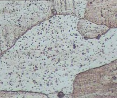
With a power of 900W, a welding speed of 30mm/s, and a defocus amount of 0mm for the fiber laser, the metallographic microstructure in the central area of the weld under different semiconductor laser powers is shown as in Figure 7,when the semiconductor laser power is set at 0W, 600W, and 800W respectively, the metallographic micrograph of the microstructure in the center of the weld is shown in Figure 7(a), Figure 7(b), and Figure 7(c) accordingly,all are equiaxed grain structures, as the power of the semiconductor laser increases, the quantity of equiaxed grain structures gradually increases. This is because the increase in the power of the semiconductor laser causes the overall temperature in the weld center to rise, providing sufficient time for the equiaxed grain structure to develop.When the power of the semiconductor laser is further increased to 1000W, the microstructure in the center of the weld transitions to large α-Cu grains, as shown in Figure 7(b). This is due to a decrease in the temperature gradient at the weld center, which causes the cooling rate of the weld to slow down significantly, facilitating the formation of large α-Cu grains.
|
(a) The semiconductor laser power is 0W |
(b) The semiconductor laser power is 600W |
|
(c) The semiconductor laser power is 800W |
(d) The semiconductor laser power is 1000W |
|
Figure 7 Microstructure of the central area of the weld seam under different semiconductor laser powers |
|
2.3 Effect of semiconductor laser on mechanical properties of welds
With the power of the fiber laser set at 900W, a welding speed of 30mm/s, and a defocusing amount of 0mm, the microhardness under different semiconductor laser powers is shown in Figure 8. As the power of the semiconductor laser increases, the maximum hardness of the weld gradually decreases. This is because the increase in semiconductor laser power extends the cooling and solidification time of the melt pool, allowing the grains to fully grow. The larger grain size results in a reduction of the material's microhardness value.The trend from the weld area towards the base material exhibits an initial decrease followed by an increase, with the maximum microhardness observed in the center area of the weld. This is due to the presence of very small grains in this area, as the grain refinement results in increased hardness.The minimum microhardness value occurs in the heat-affected zone. This is because the heat-affected zone is in the direction of heat conduction; the small temperature gradient leads to relatively larger grains, which in turn reduce the microhardness.
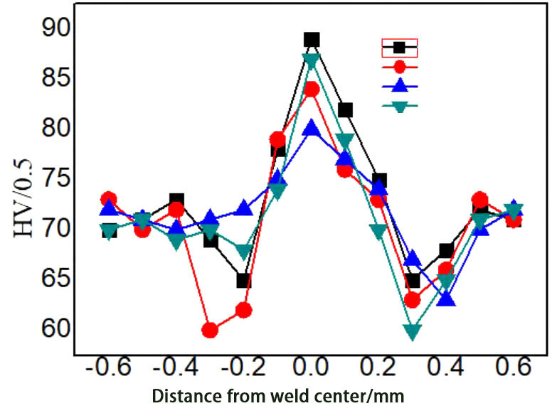
Figure 8 Microhardness distribution of welded joints under different semiconductor laser powers
3 Conclusion
Compared to traditional laser welding, preheating or surface treatment of copper is not necessary. Using fiber and semiconductor composite lasers, copper can be welded in one step, reducing the manufacturing process and saving production costs. This provides a valuable technical reference for actual production.
During the welding process, the semiconductor laser provides auxiliary heating to the weld, producing the highest tensile strength in the weld with no porosity when the power is set at 800W.The power of the semiconductor laser significantly affects the microstructure of the weld. As the power of the semiconductor laser increases, the cellular crystal structure in the fusion zone gradually becomes coarser; the grain size in the heat-affected zone increases; and the equiaxed crystal structure in the center of the weld increases in particle size. The larger grain size will reduce the microhardness of the weld.
 EN
EN
 AR
AR CS
CS NL
NL FR
FR DE
DE IT
IT JA
JA KO
KO PL
PL PT
PT RU
RU ES
ES UK
UK TH
TH TR
TR